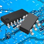
What is a ceramic-based high power LED
A ceramic-based high power LED package is a high flux density light source that operates at a minimum of 1 watt and produces a large volume of lumens from a small light emitting surface (LES). The ability to handle not only high drive currents but also high thermal loads lends high power LEDs to a broad spectrum of outdoor, indoor, architectural and portable lighting applications where the need for reliability and robustness of the light source runs parallel with the requirement for light output and energy efficiency. Delivering both high lumen output and high luminous efficacy in a small footprint, ceramic-based high power LEDs are the universal choice of light source for products demanding tight beam control and powerful illumination. The large portfolio of lighting products that rely on their dependable performance and high optical power can range from high bay lights, low bay lights, directional accent lights, high mast lights, street lights, flood lights, wall packs and landscape lights to automotive headlights, bike headlights, flashlights and torches.
Light emission
LEDs or light-emitting diodes emit light due to the injection electroluminescence effect occurring in semiconductor p-n junctions. The p-n junction is composed of an N-type semiconductor layer and a P-type semiconductor layer which are doped with donor dopant atoms and acceptor atoms to produce negatively charged electrons and positively charged holes, respectively. Sandwiched between two oppositely doped semiconductor layers is an active layer of semiconductor material from where light is emitted. When a forward voltage is applied across the doped layers, electrons jump across the boundary layer of the p-n junction and holes injected from the p-region move across the boundary layer. Intracrystalline recombination of these electrons and holes in the active layer results in the electrons falling into a lower energy level from the conduction band to the valence band. The excess energy is released in the form of electromagnetic waves which are projected outwards as light.
LED packaging
A semiconductor p-n junction is essentially a light-emitting stack known as an LED die or LED chip. Electromagnetic radiation from electroluminescence has a narrow spectrum that causes the visible light to appear in a single color. The light-emitting stack is a self-heating element which introduces thermal energy generated from non-radiative electron-hole recombination to the p-n junction during operation. Heat accumulation can raise the operating temperature, which in turn accelerates kinetics of temperature-induced degradation. The performance and service life of the light-emitting stack are also strongly influenced by environmental conditions such as humidity, corrosive atmosphere and thermo-mechanical stress. To be useful as a light source that can be installed into a lamp or luminaire, an LED die must be integrated into a package which enables technology-to-application transformation. An LED package facilitates the interconnection of the LED die to the system for power supply and thermal management, provides spectral modifications to achieve the required color characteristics, and exercises control of environmental conditions to avoid extrinsic failures.
Package construction
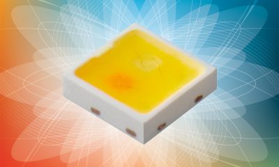
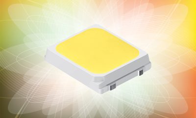
A high power LED package is engineered to address challenges unique to semiconductor emitters that operate at a high power density. It builds upon a platform that minimizes the length of the thermal path and thermal resistance in the path from junction to the printed circuit board while also maximizing the effective surface area of the interconnects and the thermal stability of package materials. This contrasts with mid-power LEDs of which the platform is evolved from the plastic leaded chip carrier (PLCC) type of electronic packages. Mid-power LEDs make use of a molded plastic housing with a reflective cavity to improve light extraction efficiency. The plastic package is inherently of high thermal resistance and low thermal/photo stability. Irreversible chemical bond breakages or rearrangements through mechanisms such as chain scission and oxidation lead to discoloration of the reflective cavity and consequently cause color shift, lumen depreciation, and shortened useful life. High power LED packages are constructed with minimized failure points and substantially improved reliability. Instead of using the vulnerable carrier system formed by a corrosion-prone lead frame and degradation-prone polymer housing, a high power LED takes advantage of a ceramic substrate and higher performance interconnects which are both high operating temperature and high drive current capable.
Influences of lattice defects on die performance
LED operation is interdependent upon thermal management and drive current regulation. Temperature-dependent semiconductor properties cause non-radiative recombination and carrier loss when an LED is operated at a temperature beyond its safe limit. Thermal droop (reduction in the optical power) occurs as it is operated at the elevated temperature. Growth of intracrystalline defects can be sped up at higher junction temperatures. Over time, the chip degeneration ends up in a substantial loss in quantum efficiency. Similarly, LEDs suffer from efficiency droop when they are driven with an injection current density beyond the point at which the maximum injection efficiency is attained. During the non-radiative recombination, the electron transition from the conduction to the valence band generates vibrational energy of lattice atoms, which is converted to heat. Increased thermal load in turn elevates the junction temperature and eventually overheat the light-emitting stack. Inadequately designed LEDs may develop excessive variations in the magnitude of thermal resistance across the die active region. When operated at high drive currents, local heating caused by current crowding will pose risks of thermal runaway. High power LEDs draw a massive amount of electrical power that can be as high as 10+ watts. The interaction between the drive current and junction temperature imposes special considerations in the design of high power LED packages.
Package submount
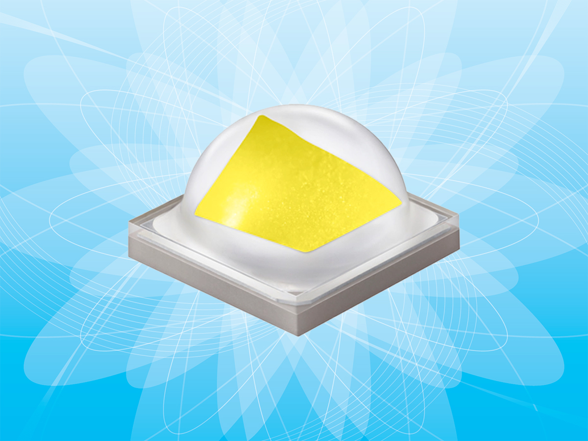
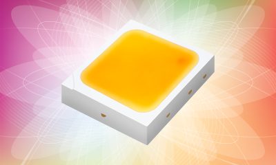
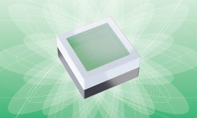
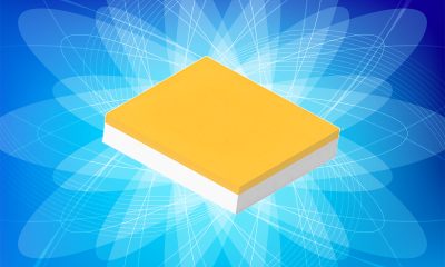
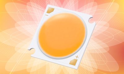
A ceramic-based high power LED package attaches a large LED die or multiple LED dies to a metallized ceramic substrate. The ceramic substrate has through-holes that connects the die or die assembly to cathode and anode pads on the underside of the ceramic substrate. These through-holes, which are filled with copper during the thin-film processing, also serve as thermal vias which provides a high efficiency thermal path to draw heat away from the LED junction. An electrically insulated thermal pad may be provided additionally to improve the thermal performance of the substrate. Ceramics are excellent thermal conductors and electrical insulators. They also offer high resistance to photo-degradation and extreme thermal stresses. Another strength of ceramic substrates is the immunity against adverse environmental conditions such as humidity, corrosive gas and air pollutant exposure. The ceramic substrate can be produced from aluminum oxide (alumina) with thermal conductivity in the range of 20-30 W/mK or aluminum nitride (140-180 W/mK). The LED die is bonded to the ceramic substrate using a high temperature, lead-free solder. The metal pads are reflow soldered to a metal core printed circuit board (MCPCB). The increased footprint of the solder interconnects not only facilitates thermal transfer between the LED packages and PCB, but also contributes to high reliability electrical connection that is critical to high vibration and shock applications. A phosphor conformal coating is spread over the LED die. A clear silicone dome lens may be molded over the LED to improve light extraction. A transient voltage suppressor (TVS) chip may be installed to protect the LED from electrostatic discharge (ESD).
Die fabrication
The package construction in general drives the lighting performance and long term behavior of the LED package. Nevertheless, the die construction makes a significant difference in the case of high power LED packaging. The p-n junction semiconductor die of a phosphor-converted white LED is a gallium nitride (GaN) system that has a double heterojunction (DHJ) structure. The active region employs quantum wells to trap positive and negative charge carriers. A quantum well is a semiconductor layer made from indium gallium nitride (InGaN), a mix of GaN and indium nitride (InN). A typical III-nitride light-emitting stack has a n-doped GaN layer at the bottom, an InGaN layer in the middle and a p-doped GaN layer at the top. The wavelength of photons released through electron transition, and thus the color of the emitted light, is governed the semiconductor bandgap, which is the difference in energy between the conduction band and valence band. The bandgap can be manipulated by adjusting the GaN/InN ratio and the thickness of the InGaN layers which are only a few nanometers thick.
Substrate technology
The n-GaN/InGaN/p-GaN heterojunction is grown on a carrier wafer. The great majority of InGaN LEDs are based on heteroepitaxial growth using foreign substrates such as sapphire, silicon carbide (SiC), and silicon (Si). But heteroepitaxial GaN growth suffers from lattice mismatch which results in a high density of defects in the crystalline structure known as threading dislocations (TDs) in the active region of the diode. High concentration of dislocations can reduce the mobility of charge carriers and the lifetime of minority charge carriers. Such defects serve as non-radiative recombination centers and generate heat rather than light. What is even worse is that TDs are the source of poor reliability of the semiconductor dies under electrical and thermal stresses. The existence of an existing defect in the crystalline structure leads to inhomogeneous thermal conduction across the active region, which can accelerate the atomic defect growth at higher temperatures. Electromigration of contact metals through the hollow center of the dislocation creates an ohmic resistance path between the P and N regions of the die. The increase in the parasitic series resistance can result in increased reverse leakage currents and poor power density uniformity, giving rise to current crowding, local heating and thermal runaway.
GaN-on-SiC vs. GaN-on-sapphire
The speed at which lattice defects spur nucleation and more crystalline defect formations in the epitaxial layer structure of the die depends on the magnitude of temperature and current. The high-power LED architecture produces the most thermal and electrical stresses to the light-emitting stack. High quality epitaxial growth is therefore critical to quantum efficiency and longevity of the LEDs. Heteroepitaxial growth of high-power GaN-based LEDs is usually performed on sapphire substrates which offer an advantage in scalable and cost-effective production. The lattice mismatch between sapphire and GaN is 16%, which is considerably large for high power applications. Silicon carbide (SiC) has a number of advantages over sapphire. The lattice mismatch for GaN-SiC pair is 3.1%, which means a significantly lower TD density. SiC has a much higher thermal conductivity coefficient than sapphire (3.8 Wt/cm K vs. ~ 0.25 Wt/cm K) and a more closely matched coefficient of thermal expansion (CTE) with GaN. These properties enable fabrication of LED dies that can be driven at higher power densities and operating temperatures than dies grown on competing sapphire substrates. GaN-on-SiC LEDs are less susceptible to electrostatic discharge (ESD) and electrical overstress (EOS). Moreover, SiC also has a better refractive index (RI) match with GaN, which results in more light extraction. These advantages combine to give a GaN-on-SiC LED a 5 to 10% efficacy advantage over GaN-on-sapphire LEDs as well as a longer service life. Of course, there is nothing better than homoepitaxial growth GaN on a substrate of the same material. The challenge to making GaN-on-GaN LEDs is the mass production of adequately sized GaN substrates at an affordable cost.
White light generation
The spectral power distribution (SPD) of an LED die has a bandwidth of about 10-30 nm. Visible electromagnetic radiation in a narrow spectral range is perceived as monochromatic light that has a single color such as red, green or blue. Phosphor down-conversion is the most abundantly used technology in spreading monochromatic light produced by an LED in wavelength to polychromatic white light. The highest efficiency white LEDs today are blue-pump LEDs in which an InGaN blue LED is coated by a phosphor layer. The phosphor down-converter absorbs a portion of the short wavelength photons and Stokes shifts them into photons of longer wavelengths. Phosphor-converted photons and blue photons that pass through the phosphor layer without undergoing a down conversion process blend together to form white light. White LED light can also be produced by completely converting the electroluminescence with an near-ultraviolet (UV) LED chip that is coated with RGB phosphors. Full conversion of the electroluminescence results in high color rendering light that delivers balanced amounts of radiant power in different parts of the visible spectrum. However, violet-pump LEDs are less efficient than blue-pump LEDs because they convert all of the short wavelength light to longer wavelength light and thus encounter more Stokes losses.
A white LED can be characterized by its correlated color temperature (CCT) and by its color rendering index (CRI). The application of phosphor down-converters to achieve high quality white light of the specified color characteristics requires careful control of material composition and layer thickness. Due to Stokes shift and light absorption, the temperatures of the phosphor layer can easily be 30°C to 50°C higher than the junction temperature of the LED. Phosphors and binder materials can also degrade, resulting in cracking and delamination. Hence the phosphor layer must be high temperature stable and have high thermal diffusivities. It is also expected to have high RI and CTE matches with the LED die, high resistance against photo-degradation, and strong adhesion and bond strength.


Loading...