
General description
High power automotive LEDs deliver high lumen output, high flux density, high efficacy and high reliability to meet requirements of automotive front lighting applications. Automotive lighting is all about visibility and reliability. The high luminance LEDs pack a powerful punch to illuminate the road ahead, allowing vehicle drivers to identify all safety hazards on the road. Lumen density is necessarily very high in these semiconductor packages. Emanating high flux from a small area, automotive LEDs afford tight beam control for precision lighting, which allows headlights to illuminate specific areas of the road without causing discomfort, distraction, or glare to other road users. Yet all this brilliant illumination is useless if the light source can’t withstand whatever the vehicle, the road, or nature can throw at them. Automotive LEDs must be engineered to hold up against high thermal and electrical stresses, face up to all expected vibration and mechanical shock, and stand the test of time.
Automotive forward lighting
LEDs are elements foundational to the lumen performance, beam characteristics, look and form, and longevity of an automotive headlighting system. The broad concept of automotive headlighting applies to lighting systems that provide forward visibility. They include high beam lights, low beam lights, driving lights and front fog lights. The “high beam”, also called a “main beam”, “upper beam”, “full beam” or “driving beam,” provides a center-weighted distribution of light that gives priority to ensuring a field of view for the driver and clearly illuminates objects ahead for a distance of up to 500 feet. The high beam is mainly used on a road with few oncoming vehicles or to give drivers a sufficient braking distance or reaction time to avoid risky operations when a vehicle is running at high speed. The low beam (sometimes called a “dipped beam”, “passing beam”, or “meeting beam”) is intended for use when other vehicles are present ahead. The downward beam illuminates about 130 feet ahead, with a cutoff line at an upper end portion of the irradiated region to limit projection of light towards the eyes of other road users. A motor vehicle may be equipped with auxiliary driving lights to supplement the high beams. They illuminate an area further and wider than what the high beams are capable of to spot obstacles in the distance. These forward lighting systems are commonly used in off-road lighting applications. Front fog lights are mounted below the headlights to a wide path of light for clearer visibility in fog, rain, snow, or dust.
LED technology ushers in a new era of automotive lighting
Solid state lighting is at the heart of recent innovation in the automotive lighting industry. The monumental transition to LED lighting has been propelled by the profound energy, performance, design and application benefits delivered by this technology. The luminous efficacies of high power white LED packages are approaching 200 lm/W for cool white, which lead to a significantly reduced load on the vehicle electrical system. Controlling the light distribution from the light source is just as meaningful as how much light is generated and at what efficacy. With a small footprint, high flux density and optical directionality, LEDs allow the use of small secondary optics to extract photons directly from the source and precisely direct them through key vertical and horizontal planes, without the need for large reflectors. Greater control over the light distribution and minimized optical system enable more freedom in new headlighting form factors that enhance the styling and aerodynamic design of a vehicle. The spectral power distribution (SPD) of LEDs can be engineered to provide optimal visibility on the road. With full dimmability and electrical switch durability, LEDs bring lighting to the forefront of controllability. The instantaneous response to on/off switching control presents a significant safety advantage. LEDs emit light from a small block of semiconductor, rather than from a vacuum or gas tube, as is the case in traditional halogen and HID light bulbs. The solid state durability makes them far more tolerant of shock, vibration, and mechanical stresses.
How do LEDs work
An LED produces luminescence under electrical influences. The electroluminescence takes place in a p-n junction formed by introducing impurities into two layers of single-crystal semiconductor material. One of the semiconductor layers incorporates acceptor impurity atoms to produce an n-region that generates negatively charged electrons. The other semiconductor layer is doped with donor impurity atoms to create a p-region in which the majority carriers are positively charged holes. Sandwiched between the two oppositely doped layers is the active region from where light is emitted. When a forward voltage is applied across the p-n junction, electrons in the n-type semiconductor layer and holes in the p-type semiconductor layer are forced into the active region. When an electron meets a hole, the electron drops from the higher-energy band of orbitals (conduction band) to the lower-energy band of orbitals (valence band), releasing excess energy in the form of a photon. The wavelength of the emitted photon, and hence the color of light, is determined by the semiconductor bandgap, which is the energy gap between valence-band electrons and conduction band electrons.
LED packaging
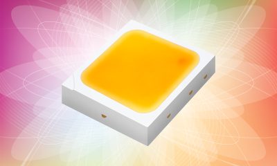
A p-n junction semiconductor die relies on a packaging structure to play its role. The electroluminescence emitted by the bare LED die have typical spectral bandwidths of a few tens of nanometers. The narrow-band emission appears to have a monochromatic color such as red, green or blue. To create white light from the narrow-band emission, wavelength conversion to broaden the light spectrum must be performed. One of the objectives of LED packaging is to provide spectral modification for the monochromatic emitter. LED devices are temperature-sensitive and current driven. Their performance and lifespan are very much at the mercy of the interdependent electrical (current, voltage, power) and thermal (junction temperature) characteristics. For automotive headlighting applications where high thermal and electrical loads are present, a high capacity thermal path and robust electrical connections must be provided through semiconductor packaging. A semiconductor package provides the LED die interconnectivity for direct surface mount technology (SMT) connection to a printed circuit board (PCB). The package is also a housing that surrounds the semiconductor die to provide environmental protection.
Package design
A handful of options currently exist for LED packaging. The package design and construction drive the power density, luminous efficacy and long-term behavior of a semiconductor emitter. Generally, a high power LED package designed for automotive headlighting applications includes an SMT submount, an LED die arranged on the submount, and a phosphor matrix formed on the die to provide encapsulation and wavelength conversion. Typically, the submount in a high power automotive LED is a ceramic substrate. The two sides of the p-n junction, the anode (+) and the cathode (-), are connected to the package’s electrical contacts through wire bonding or wire-free connection. A high power automotive LED package may be a single-emitter device or a multi-emitter device. A single-emitter device has one pair of electrodes, whereas a multi-emitter device has a dedicated pair of electrodes for each emitter. Die construction and package design go hand in hand. The performance of a semiconductor die under the expected operational stresses defines the maximum values for junction temperature and current density, which in turn determine the choice of package architecture and materials.
Die fabrication
A pump LED, which is an LED die used to produce primary light for subsequent wavelength conversion within the semiconductor package, is formed in epitaxial layers and made of gallium nitride (GaN). GaN is a III-V-nitride compound semiconductor with a direct and wide banggap, in addition to high thermal and chemical stability. Semiconductor emitters with a direct band gap have a high internal quantum efficiency because the energy transition in electrons releases photons directly without requiring a shift in the k-space. A wide bandgap allows GaN devices to be operated at higher power and higher efficiency than semiconductor devices with a narrower bandgap. The light-emitting stack of a GaN-based pump LED is a double heterojunction (DHJ), in which a lower bandgap active layer made from indium gallium nitride (InGaN) is sandwiched between the p-GaN layer and n-GaN layer. The nanometer-thin InGaN layer provides a quantum well (QW) based active region that enables efficient confinement of both electrons and holes. The wavelength of emitted light is tuned by varying the active layer thickness and the amount of indium in the InGaN alloy.
Substrate technology
The performance and efficiency of InGaN LEDs have a strong dependence on the substrate technology used for GaN epitaxial growth. The substrate choice dictates the quality of the semiconductor crystalline structure. Nothing beats homoepitaxial growth of GaN stacks on GaN substrates due to the 100% coefficient of thermal expansion (CTE) and lattice matches between the light-emitting stack and carrier wafer. However, massive production of GaN-on-GaN LEDs at an affordable cost remains a challenge. Heteroepitaxial growth of GaN is currently carried out on foreign substrates, which inevitably results in defects in the crystalline structure. A lattice mismatch between GaN and these substrates can result in threading dislocations (micropipes or nanopipes) forming at the interface. The presence of threading dislocations reduces probability of radiative recombinations between electrons and holes at these sites, which causes a reduction in quantum efficiency. Thread dislocations affect the electrical properties of GaN. A high dislocation density increases reverse leakage currents, brings down breakdown voltage, and leads to inhomogeneous distribution of the current density. At high drive currents and operating temperatures, these failure mechanisms can accelerate the kinetics of atomic defect growth, result in current crowding and local heating, and eventually lead to thermal runaway and die cracking.
GaN-on-SiC vs. GaN-on-sapphire
By far GaN epitaxy is most often grown on sapphire substrates. Unless there are effective thermal management and tight drive current regulation, GaN-on-sapphire LEDs will not perform to their full capacity in a very challenging operating environment. Automotive headlighting applications typically require the light sources to deliver a high flux density, which makes their high drive current operation a necessity and the resulting thermal load very high. The large lattice mismatch between GaN and sapphire results in a high density of threading dislocations that leads to a significantly reduced light output at high operating temperatures and a shortened useful life. Compared with sapphire, silicon carbide (SiC) has a closer lattice match to GaN, higher thermal conductivity, simpler nucleation layer structure and better refractive index matching (RIM) of GaN to the substrate. These advantages lend GaN-on-SiC LEDs supremacy over GaN-on-sapphire LEDs. GaN-on-SiC LEDs can operate at higher operating temperatures and drive currents without compromising lumen performance and long-term reliability. An additional benefit is that they are less susceptible to electrostatic discharge (ESD). In contrast, GaN-on-sapphire LEDs are easily damaged by ESD and thus require special packaging and careful handling. A transient voltage suppressor (TVS) chip is usually integrated into the submount to protect the LED die against ESD events.
Die integration
In a conventional high power LED package, the LED die is mounted to the submount in a way that the die substrate is at the bottom. In this orientation, the electrical connection to the epitaxial p-GaN layer has to be made using wire bonding. Shock, vibration, voltage fluctuations, corrosive atmosphere, and extreme temperatures are regular occurrences that automotive LEDs are exposed to. Wire-bonded electrical connections are vulnerable to corrosive attack and mechanical influences. When LED dies are exposed to high forward currents or high peak transient currents, the electrical overstress (EOS) may cause a bond wire breakage and thus an open circuit failure. To maximize light extraction, the Ni/Au contact on the p-GaN layer must be made thin enough. The cost of this is a reduced carrier injection efficiency (CIE) due to current crowding. Another issue with the conventional mounting scheme is the large thermal resistance at the interface between the sapphire substrate and submount. Sapphire has a low thermal conductivity. It acts more as a thermal insulator rather than a conductor, and can impede flow of heat flux from the light-emitting stack to the submount.
Flip chip attachment
The fundamental packaging philosophy of high power automotive LEDs is to minimize thermal resistance and maximize product reliability under high operational and environmental stresses. To overcome limitations imposed by conventional package platforms, there has been a concerted effort to introduce flip chip attachment (FCA) technology into LED packaging. FCA refers to mounting the LED die with the substrate side facing up and the p-GaN layer being put face down on the submount or electrode. Light is transmitted through the n-GaN layer and die substrate. The current flows vertically through the epitaxial p-GaN layer. This configuration allows current and heat spreading on the p-GaN layer to be handled by a thick, large p-contact, which means homogeneous current distribution and high efficiency heat dissipation. The flip-chip structure eliminates the need for wire bonding, which is a single point of failure in conventional packages. The anode and cathode contacts are located on the base of the package. The n-GaN layer is connected to the bottom contact by way of a through-hole which are also used as a thermal via. Metal electrode pads on the underside of the package are designed to be reflow soldered onto a PCB. Additional thermal conduction pads may be used to facilitate heat flow. The use of large contact pads significantly drives down spreading resistance and produces higher reliability interconnects that are critical to automotive lighting applications.
White light generation
A high power automotive LED package utilizes one or more blue-emitting LED dies to pump phosphors within the semiconductor package. Part of the pump light is spectrally shifted to longer wavelength light. The remaining blue light passes through the phosphor layer without going through the down-conversion process. The subsequent wavelength blending results in a spectrum of light with a broadened spectral range, which is perceived as white light by human eyes. The exact spectrum of the pump light combined with the phosphors loading into the silicone matrix and the thickness of the phosphor matrix layer is what defines the color characteristics of the emitted white light. White light can be characterized by its color rendering performance and correlated color temperature (CCT). In terms of color rendition, automotive lighting applications tend to put more weigh on the color discrimination ability of a light source than its color fidelity. Cool white is often the color of choice for automotive lighting. Cool white LEDs have higher luminous efficacy than warm white LEDs because they suffer less Stokes energy losses during the down-conversion process. The higher blue constituent in cool white light helps simulate a daytime physiological response in the vehicle driver and other road users. However, in hazy or dusty atmospheres warmer white light tends to offer better detail and contrast.


Loading...