
General description
Automotive signaling LED packages are specifically designed for use in exterior signal lights which are attached at the front, side and rear of a vehicle to increase the visibility of the vehicle and provide information for other road users. Active and passive safety lighting goes hand in hand to reduce the risk potential for all road users. Automotive lighting is not simply about providing optimal visual conditions for the vehicle driver in low light and poor weather conditions, but also takes into account the driver’s need to be seen by oncoming and preceding vehicles, pedestrians and cyclists. Automotive signal lights are perception and communication tools designed to provide optimal vehicle visibility. They make use of visible light as a safety element to indicate the presence and size of a vehicle and allow vehicle drivers to communicating their intentions such as turning, braking, accelerating and hazard warning. These lighting devices drive a set of life-critical interactions through the influence of both static and dynamic lighting.
Automotive conspicuity, signal and identification lights
An automotive vehicle is equipped with an assortment of conspicuity, signal and identification lights to indicate its presence, size, position, direction of travel, change in direction or deceleration. Daytime running lights (DRL) are forward lighting devices that are intended to make vehicles more conspicuous to other drivers when the high beam or low beam headlights are not activated, such as during daytime or in mixed lighting conditions. Front position lights and rear position lights are used to indicate the presence and the width of a vehicle when viewed from the front and the rear respectively. End-outline marker lamps (white in front and red at rear) indicate clearly the vehicle’s overall width and complement front and rear position lights for certain vehicles and trailers by drawing particular attention to their bulk. Clearance lights and identification lights are required on multipurpose passenger vehicles (MPV), truck, and buses to indicate the overall width of the vehicle. Rear fog lights are intended to make a vehicle’s presence more easily visible from the rear in dense fog. Side marker lights allow a vehicle to easily seen and distinguished when viewed from the side. Turn signal lights are direction indicators that provide a flashing warning light to give a signal of intention to turn right or left. Brake lights, including those placed on the rear of the vehicle and the center high-mounted stop lamp (CHMSL), project red light behind the vehicle upon application of the service brake. White reversing lights (back-up lights) are used to indicate the status of a vehicle being put into reverse gear.
LED technology drives automotive lighting innovations
The automotive lighting industry has been undergoing a radical transformation fueled by the groundbreaking advances introduced by the LED technology. The new technology offers a huge opportunity to improve the performance, functionality and value of automotive lighting. LED lighting offers very significant savings and provides longer lasting operation compared to all conventional lighting technologies. The new technology offers a standard of safety never achieved in the past. LEDs have a virtually instantaneous response time in the nanoseconds range. The time they take to rise to full intensity is about 10 times faster than incandescent lamps. The faster response time of LED brake lights results in a gain in valuable meters of braking distance for vehicles running at a high speed. LEDs can be spectrally engineered to emit light in any color, which makes it possible to address regulatory color requirements at the source level without using colored lenses. The excellent dimmability, electrical switch durability and additive color reproduction ability of LEDs allow an infinite variety and combination of dynamic effects to be used as warning functions. LED lighting adds a new dimension to vehicle styling and facilitates new design trends in cars. With small footprints and optical directionality, LEDs make lighting an integral part of the design signature of a car and afford automotive stylists the chance to advance beyond legacy form factors of automotive exterior lights.
How do LEDs work
LEDs are semiconductor devices which convert electric power directly to visible light by exciting electroluminescence (luminescence under electrical influences) in a p-n junction. The semiconducting p-n junction comprises an active region sandwiched between an n-type semiconductor layer and a p-type semiconductor layer. When a forward voltage is applied across the p-n junction to overcome reverse electric field at the junction between the two oppositely doped semiconductor layers, electrons and holes move across the n-junction and the p-junction respectively into the active region. These electrons and holes recombine with each other in the active region to generate light as a result of energy transition in electrons. The intracrystalline recombination of the charge carriers causes the negatively charged electrons to fall from the conduction band to the valence band and release excess energy in the form of photons which are discrete bundles of light.
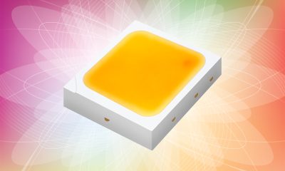
LED packaging
Automotive signaling LED packages are application-level devices that build upon the p-n junction semiconductor dies. Semiconductor packaging serves many important functions for the LED die which is essentially a light-emitting stack. The package structure allows the light-emitting stack to be electrically, thermally and mechanically interfaced to a printed circuit board (PCB) through standard surface-mount technology (SMT). LEDs rely on semiconductor packaging to construct a robust thermal path because the thermal energy generated during operation is directly dissipated from the LED junction through conduction rather radiation as seen in incandescent sources. Both the thermal path and electrical connections to the PCB depend on the mechanical integrity of the interconnects between the package and PCB. Automotive LEDs can be subjected to high mechanical stresses due to repetitive, high-magnitude temperature cycling and vibration. The LED package must be designed to facilitate a high reliability interconnection at the interface. The package into which LED dies are incorporated also has a function of protecting them from environmental contaminants. Most automotive LEDs that are intended for conspicuity, signal and identification lighting are white-emitting devices whereas the p-n junction semiconductor dies emit light in a narrow spectral range. An LED package therefore needs to perform wavelength conversion to spectrally modify the electroluminescence in order to emit white light with the required spectrum.
Package design
The package design drives the mechanical, electrical, thermal, and optical performance of an LED as well as its long-term behavior. A typical automotive LED package has a carrier, one or more LED dies, and an encapsulant. The package carrier is the SMT submount where the LED dies are mounted and the interface between the package and PCB is created. The package platform for most low- and mid-power LEDs has been evolved from the plastic leaded chip carrier (PLCC) type of electronic packages. An SMD LED based on this platform has one or two small dies mounted onto a metal lead frame which is then embedded in a polymer cavity and filled with a phosphor containing encapsulating matrix. The lead frame creates one of the electrical connections to the LED die. The other one is connected electrically by a bond wire. Polymer-based LEDs allow only a limited level of power density because decomposition behavior of the plastic housing is very common when they’re driven at high drive currents. Higher power lighting applications conventionally resort to ceramic-based LED packages which create a high efficiency thermal path by mounting the LED die on aluminum nitride (AlN) ceramic submounts and using metal contact pads to facilitate the interconnection of the LED to the system.
Die fabrication
Every package design revolves around the performance characteristics of the LED die. LED dies are formed in epitaxial layers which are fabricated from a single-crystal semiconducting material. Acceptor impurity atoms are incorporated into one of the single-crystal semiconductor layer to produce the p-region in which the majority charge carriers are holes. The other single-crystal semiconductor layer is doped with donor impurity atoms to produce the n-region where the majority charge carriers are electrons. The active region is made from a lower band gap material, which is usually an alloy based on the single crystal. The wavelength of emitted light is determined by the semiconductor bandgap, which is the energy difference between conduction band electrons and valence-band electrons. Direct bandgap semiconductors are preferred over indirect bandgap semiconductors because they allow direct radiative electron-hole recombination and thus a higher carrier radiative recombination efficiency (RRE). Gallium nitride (GaN) has been the material of choice for fabricating high efficiency white, green, cyan, blue, and royal blue LEDs due to its direct and wide bandgap. A GaN-based LED is a n-GaN/InGaN/p-GaN heterojunction. The active layer of indium gallium nitride (InGaN) creates a quantum well based active region that promotes high efficiency radiative electron-hole recombination. When there’s a requirement to produce red, deep red, red-orange, and amber light from the LED die, the less efficient aluminum indium gallium phosphide (AlInGaP) material system has to be used.
Substrate technology
The epitaxial light-emitting stack is grown on a carrier wafer (die substrate). Substrate technology establishes the fundamental capabilities of an LED. AlInGaP LEDs can be grown on gallium arsenide (GaAs) substrates which have a close lattice match to gallium phosphide (GaP). However, the lighting industry has been struggling with finding a cost-effective, high-quality substrate for GaN epitaxy. InGaN LEDs are predominantly fabricated through heteroepitaxial growth on foreign substrates. Heteroepitaxy results in mismatch between the crystal lattice structure of the substrate and that of InGaN. A lattice mismatch introduces a defect in the crystalline structure such as a threading dislocation. At the place where a crystalline defect is present, electron-hole recombination often does not result in the generation of light. A high dislocation density will not only cause optical power degradation, but also increase reverse leakage currents in the active region and result in inhomogeneous current distribution. At high drive currents and high operating temperatures, the crystalline defect generation and growth can be accelerated at high magnitude in lattice-mismatched LEDs. The interaction between the crystalline defects and operational stresses eventually leads to a massive reduction in light output and premature device failures. Sapphire has established itself as the substrate of choice for heteroepitaxial growth of GaN. However, its large lattice mismatch to GaN leads to an exponential drop in quantum efficiency at high drive currents and a short service life under high operational stresses. A superior but more expensive alternative is silicon carbide (SiC). A SiC substrate has the smallest lattice mismatch to GaN among all foreign substrates, which makes GaN-on-SiC LEDs more reliable and efficient. Its high thermal conductivity contributes a low thermal resistance at the interface between the die and submount. GaN-on-SiC LEDs also have improved resistance to electrostatic discharge (ESD).
Interconnect reliability
LED packages designed for automotive lighting systems are stressed significantly by the operational and environmental conditions. They must be robust enough to thrive in an operating environment where the likelihood of electrical overstress (EOS), thermo-mechanical stresses and vibrational damages is very high. Conventional package platforms are designed in a way that the electrical connection to the p-type semiconductor layer is made through wire bonding. Wire bonding breakage is a major failure mechanism in LED packages. High electrical transients and high DC forward current can cause the bond wire to melt and interrupt the current. Temperature cycling and vibration exert mechanical stresses on wire bonding to create a wear-out failure mechanism. The Ni/Au contact on the p-type semiconductor layer must be small enough in order to extract light as much as possible. The small electrical contact can result in current crowding and inhomogeneous current spreading, which lowers the injection efficiency of the light-emitting layer. Also in conventional mounting schemes, the die substrate is made in contact with the submount. Since sapphire substrates have a low thermal conductivity, they act as a thermal insulator, rather than a conductor in this arrangement.
Flip chip attachment
Flip chip attachment (FCA) technology has made its way into LED packaging to address the deficiencies in traditional package platforms. The new package design puts the p-type semiconductor layer on the flip side to make it in direct with the bottom anode electrode. In this orientation, the substrate side faces up to become a light transmission layer. A significant advantage of this design is that the forward current can flow vertically through the epitaxial p-GaN layer. It is impossible to use a current spreader to distribute current uniformly over the full span of the LED die, which can significantly improve the electrical performance. Wire bonding connections are removed. The epitaxial n-GaN layer is electrically contacted to the bottom cathode pad via through-hole connections which simultaneously serves as thermal vias. With both electrode pads of the LED located on the base, high reliability interconnectivity can be created to ensure high efficiency thermal conduction and high current flow. High power flip-chip LEDs typically mount the LED dies on a ceramic submount to provide a latent heat capacity. Chip scale package (CSP) LEDs strip away the submount to scale down the size and minimize the thermal path.
Spectral engineering
Monochromatic color LEDs are created by varying the chemical composition and thus the bandgap of the semiconductor material that forms the active region. White light is created by using an InGaN emitter to pump phosphors within the LED package. The correlated color temperature (CCT) and color rendering property of light generated by the blue-pump LED is defined by the exact wavelength of the pump light, the composition of the phosphor down-converter, and the layer thickness. Silicone is generally used as the matrix for phosphor down-converters while providing encapsulation for the LED die. Die manufacturing and phosphor-matrix application processes play a large role in color accuracy and consistency of the packaged products.


Loading...