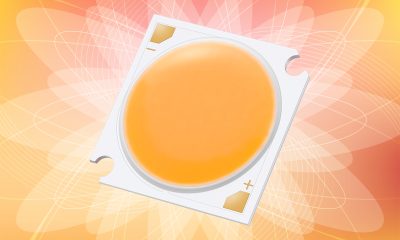
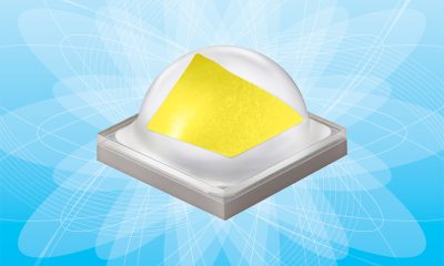
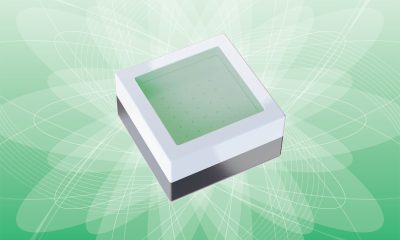
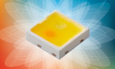
What is a mid-power LED
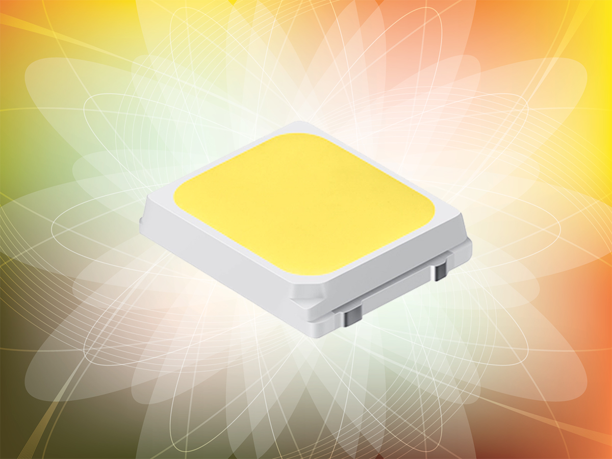
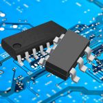
A mid-power LED is a semiconductor emitter package that operates at a maximum of 1 watt. Within the lighting industry, it typically refers to a polymer-based package that is architecturally evolved from the plastic leaded chip carrier (PLCC) type of electronic packages. PLCC packages for mid-power LEDs come in physical specifications that follow the standard nomenclature for SMT packages such as 2835 (3.5 x 2.8 mm), 3030 (3.0 x 3.0 mm), 3014 (3.0 x 1.4 mm), 5630 (5.6 x 3.0 mm), and 3535 (3.5 x 3.5 mm). Mid-power LEDs are the usual choice for residential and commercial lighting products such as ceiling lights, troffers, wall sconces, floor lamps, table lamps, GLS retrofit lamps and tubular lamps. Among all LED package types, PLCC LEDs provide the best architecture for non-directional lighting applications in residential and commercial settings. The small size supports retrofit applications and enables more freedom in new lighting form factors. The controlled environment of an indoor space and lower power designs of most indoor lighting products set the stage for these vulnerable LED packages. Moreover, their cost and efficacy advantages lend them a killer punch in the commoditized lighting markets.
LED chip (die) vs. LED package
The term “LED”, which is short for “light-emitting diode”, generally refers to the semiconductor package, and thereby differentiates from the term “LED chip” or “LED die”. An LED chip or LED die refers to the semiconducting p-n junction which is a light-emitting stack consisting of an active layer (the light-emitting element) interposed between the N-type semiconductor layer and the P-type semiconductor layer that have different modes of electrical conductivity. An LED chip cannot function independently in an application because it’s merely a semiconductor structure. The bare semiconductor die must be packaged before it can be used in an application. The package into which the semiconductor die (LED chip) is assembled plays multiple roles in that it provides electrical leads for connecting the die to an external circuit via a printed circuit board (PCB), interfaces the die thermally with the printed circuit boards, performs spectral modification for the emitted light, protects the die from being damaged physically or chemically, and also incorporates and performs optical functions.
Package construction
An LED package is generally constructed of a carrier, a die or an array of dies, an encapsulant containing a wavelength conversion material, and the p- and n-type electrodes. A mid-power polymer-based LED package is characterized with a structure wherein a metal lead frame mounted with one or more small LED dies is embedded in a polymer cavity. The polymer cavity is filled with a phosphor-polymer mixture which act as the wavelength down-converter and encapsulant. In addition to providing mechanical support, the lead frame serves as a medium for electrical connection and thermal dissipation. The die can be either attached through a silver containing glue or soldered onto the lead frame surface to create electrical connection for the cathode of the p-n junction. The anode of the LED die is connected electrically by a bond wire. Both the lead frame and plastic housing act as reflectors that maximize light extraction efficiency (LEE), allowing the LEDs to deliver the highest luminous efficacy among all package types. Lead frames are usually made from a copper alloy or a nickel iron alloy. They are often plated with silver to increase reflectivity and connectivity. When exposure to corrosive elements such as atmospheres containing corrosive sulfur compounds is a concern, gold plating is used instead to ensure the chemical stability. The polymer cavity or housing is molded from polyphthalamide (PPA), polycyclohexylenedimethylene terephthalate (PCT), epoxy molding compound (EMC), or silicone-based composites.
Light emission
LEDs are electroluminescent devices that emit light through intracrystalline recombination of holes and electrons. When a forward voltage sufficient to overcome the reverse electric field is applied across the p-n junction, electrons in the n-junction move across the depletion region (junction boundary) to fill up the holes migrated from the p-junction in the active layer. When electrons combine with holes, electrons fall to a lower energy level, releasing excess energy in the form of photons that can transport electromagnetic radiation of all wavelengths. A p-n junction is engineered from a single piece of semi-conductive crystal modified in two separate regions. One of the regions is doped with acceptor impurity atoms to form the p-region in which the majority carriers are holes. The other region is doped with donor impurity atoms to form the n-region in which the majority carriers are electrons. The wavelength of the light emitted by the p-n junction is determined by the difference in energy between the conduction band and valence band of the semiconductor active (light-emitting) layer.
Die fabrication
Gallium nitride (GaN), a direct and wide bandgap III-V compound semiconductor, is the material of choice for electroluminescent devices. The semiconductor with a direct band gap has a higher quantum efficiency of electroluminescence than with an indirect band gap. The wide band gap of GaN allows LEDs to operate at much higher power densities and operating temperatures than conventional semiconductors. A typical III-nitride LED has a n-doped GaN layer at the bottom, a quantum well (QW) based active region in the middle and a p-doped GaN layer at the top. The quantum well is fabricated from indium gallium nitride (InGaN) and has a double heterojunction (DHJ) structure. An active region is generally designed with multiple quantum wells to improve confinement properties and minimize Auger effects for improved quantum efficiency.
Substrate technology
A GaN-based mid-power LED die is generally formed by growing epitaxial layers on a substrate (carrier wafer) such as sapphire, silicon (Si), silicon carbide (SiC), gallium nitride (GaN) or gallium arsenide (GaAs). Currently, GaN LEDs which are heteroepitaxially grown on sapphire dominate the market because the sapphire substrate supports a relatively high quality GaN epitaxy and exhibits high processability in a wide range of temperatures. However, the large mismatch (~16%) between the crystal lattice structure of sapphire and that of GaN results in a high density of threading dislocations (defects in the crystalline structure). Such a dislocation density in the GaN layers can lead to reduced probability of photon generation, increased heat generation and accelerated atomic defect generation at high drive currents. Compared to GaN-on-sapphire LEDs, GaN LEDs grown on SiC substrates have a 5 to 10% efficacy advantage and higher reliability at high power densities due to the lower lattice mismatch (3.1%), fewer epi defects and better thermal conductivity of SiC. Moreover, GaN-on-SiC LEDs are less susceptible to electrostatic discharge (ESD) whereas GaN-on-sapphire LEDs are easily damaged by ESD. GaN LEDs can also be homoepitaxially grown GaN substrates. GaN-on-GaN LEDs are capable of operating at high drive currents and have higher efficiencies than those made with traditional carrier wafer materials.
White light generation
The narrow-band emissions of LED dies need to be spread in wavelength in order to produce composite white light with a desired color temperature and color rendering quality. Phosphor-converted white LEDs utilize short wavelength photons emitting from LED dies to excite phosphors which perform as wavelength down-converters to Stokes shift part or all the electroluminescence to other wavelengths. The most common white LEDs today employ the partial conversion concept. A blue-emitting LED die is used to pump a phosphor coating which converts a portion of the short wavelength light. The down-converted photons which have been shifted to longer wavelengths mix with blue photons that escape without going through a down conversion process, which results in the emission of white light. Partial conversion has the fundamental advantage of higher efficiency over full conversion, since not all electroluminescence is down-converted and thus the resulting Stokes-shift loss is relatively small. With full conversion, all primary radiation generated utilizing an ultraviolet (UV) LED is converted to secondary light by three separate RGB phosphors. The down conversion process generates a higher Stokes-shift loss. An advantage to this method is a spectral power distribution (SPD) with uniform distribution of radiant power across the visible wavelength range. The light spectrum is very well balanced to provide the most accurate color rendition.
Down-converter and encapsulant
The phosphors are spread over inside the polymer encapsulant that surrounds the LED die. Achieving white light of the specified color quality and color point requires careful control of phosphor luminescent transitions through manipulation of material composition and layer thickness. A typical phosphor, e.g., cerium-doped yttrium aluminum garnet (Ce:YAG), is a two-component system consisting of a host crystal matrix containing luminescent ionic centers. Uniform and reproducible application of the phosphor encapsulation matrix is critical to chromaticity consistency across multiple LEDs. The matrix for downconverter materials must be stable with respect to exposure to thermal stresses and high intensity blue/UV emission. Silicone is generally used as the matrix for phosphor encapsulation because of its high thermal stability, high optical transparency, high photostability, mechanical softness for preservation of wire bond, structural stability during service, and good adhesion to surfaces. The refractive Index (RI) mismatch between the polymer matrix and phosphor particles must be minimized to reduce the effects of light scattering and total internal reflection (TIR) which are two major contributors to losses in light extraction efficiency.
Luminous efficacy
The package design drives the efficiency of the semiconductor devices. Internal quantum efficiency (IQE) losses of polymer-based LEDs are often a consequence of efficiency droop due to operation at higher current density and high junction temperatures. When the drive current and junction temperature are maintained at their optimums, polymer-based mid-power LED LEDs outperform the competition due to their high light extraction efficiency (LEE). Utilizing the improved PLCC package platform, luminous efficacies of cool white LEDs can be as high as 240 lm/W and warm white LEDs can deliver an efficacy of up to 210 lm/W. The reflective polymer cavity and lead frame allow efficient extraction of light that would otherwise be trapped inside the LED package due to TIR at the interface between the LED die and the phosphor conversion layer and at the interface between the phosphor conversion layer and air. Approximately 13% primary radiation generated by the LED die and an equally significant portion of white light are not extracted out of a typical LED package with no light extraction designs.
Lumen maintenance and color stability
The package construction determines long term behaviors (lumen maintenance, color stability, reliability) of LEDs. Although mid-power LEDs can initially generate a higher amount of lumens per watt, the irreversible decay in external quantum efficiency (EQE) tends to accelerate as the devices are stressed at high temperatures and/or high drive currents. Another important issue concerning these LEDs is chromaticity point stability. Mid-power LED packages have a high probability of color shifts. Discoloration of the temperature-sensitive and photo-reactive plastic housing is a dominant mechanism for lumen depreciation and color shift in mid-power packages. The most prevalent materials for molding the reflective LED housing are PPA and PCT. They are susceptible to photo-oxidation and thermal degradation. These materials are usually limited to use in LED packages that operate at less than 0.7 W. Higher power packages require the use of materials, such as EMC, that have an improved resistance to discoloration. Other factors can lead to lumen depreciations and color shift. They include oxidation of exposed lead frames, phosphor delamination and degradation, and silicone micro-cracks or yellowing. Interconnect-related failure mechanisms of mid-power LEDs also demand attention throughout the package design. Wire bonding breakage due to electrical overstresses or temperature cycling is indeed a fair likelihood.


Loading...