What is a monochromatic color LED
A monochromatic color LED is a semiconductor light source that emits light in the color of a single hue. Its narrow-band emission results in a perceptual response of colored light such as red, green, blue, amber, cyan, far red, deep red, red-orange, and royal blue. Monochromatic emitters are used for creating colorful luminance to make visual sense to the viewer, rendering color peaks in the desirable attributes of the illuminated objects, or engaging a specific response. There is an almost infinite range of lighting applications that call for the distinctive spectrum of color LEDs. Color LEDs are used to bring the luminous splendor of LED technology to architectural facades and landmarks, to transform a landscape into a captivating and inspiring environment, to enhance the aesthetic appearance of an interior space, and to breathe all the drama and excitement of stage lighting into audiences. The world of horticulture lighting is growing by leaps and bounds with color LEDs being used to drive photosynthesis and regulate physiological processes such as photomorphogenesis, photoperiodism, and phototropism.
Light emission
Monochromatic color LEDs take advantage of electroluminescent effects in semiconductor p-n junctions to emit light with specific spectral bandwidth. A semiconductor p-n junction is an LED die (LED chip) constructed from two oppositely doped semiconductor layers and an interposed an active region of semiconductor material. One of the semiconductor layers is doped with acceptor impurity atoms to produce the p-region in which the majority carriers are positively charged holes. Donor impurity atoms are incorporated into the other semiconductor layer to produce the n-region in which the majority carriers are negatively charged electrons. When a forward voltage is applied across the p-n junction to overcome the reverse electric field and drive electric current, electrons in the n-type semiconductor layer and holes in the p-type semiconductor layer move across the junction boundaries into the epitaxial active region which is sandwiched between the two oppositely doped layers. Light is emitted from the active region upon the intracrystalline recombination of these holes and electrons. This effect is referred to as injection electroluminescence, which is defined as luminescence (spontaneous emission of light by a substance not resulting from heat) arising from electrical influences.
Spectral control
The injection electroluminescence occurs as a result of energy transition in electrons when they recombine with holes. The electrons drop down from the conduction band to the valence band and release their excess energy in the form of photons which are quanta of radiant energy. By manipulating the semiconductor bandgap, these photons can transport monochromatic electromagnetic radiation throughout the entire visible spectrum. The semiconductor bandgap refers to the difference in energy between the conduction band and valence band. It is determined by the chemical composition of the semiconductor material from which the light-emitting stack (the p-n junction) is fabricated. The desired emission wavelength of an LED and, consequently, the color of emitted light can be generated by using a semiconductor material with the appropriate energy bandgap. Preferably, the semiconductor material should have a direct and wide bandgap. Direct bandgap semiconductor emitters have a higher quantum efficiency than indirect bandgap semiconductor emitters due to the direct radiative recombination during energy transition. In an indirect bandgap device, a photon cannot be directly produced because the excited electron must pass through an intermediate state in the k-space and then transfer momentum to the crystal lattice. A wide bandgap allows the LED die to operate at high voltages, frequencies, and temperatures.
Material system
Monochromatic color LEDs generally fall under either the Indium Gallium Nitride (InGaN) family or the Aluminum Indium Gallium Phosphide (AlInGaP) family. An InGaN LED capitalizes on the direct and wide bandgap of gallium nitride (GaN), a III-V-nitride compound semiconductor. The light-emitting stack is typically designed as a n-GaN/InGaN/p-GaN heterojunction in which the quantum-well (QW) based active region is made of a mix of GaN and indium nitride (InN). By varying the amount of indium in the InGaN alloy, the bandgap can be tuned to produce green, cyan, blue, or royal blue light. The quantum efficiency of electroluminescence in InGaN light-emitting stacks is very high in the blue portion of the light spectrum. Increasing the indium composition to produce electroluminescence in the green spectral region results in a rapid reduction in efficiency. All red, deep red, red-orange, and amber LEDs are currently fabricated from the AlInGaP material system. The wavelength of light is tuned by adjusting the indium composition in the active layer. Gallium phosphide (GaP), however, has an indirect bandgap. A diminishing internal quantum efficiency at shorter wavelengths can be expected because of the lack of current confinement as a result of the direct-to-indirect bandgap crossover. AlInGaP LEDs have a high thermal efficiency droop and a low extraction efficiency due to the higher index of refraction. All these deficiencies lead to a very low external quantum efficiencies in a finished package.
Substrate technology
The light-emitting stack formed in an epitaxial layer is grown on a carrier wafer (die substrate). Heteroepitaxial growth of GaP on GaAs substrates yields highly lattice-matched AlInGaP LEDs. Heteroepitaxial growth of GaN for InGaN LEDs can be performed on sapphire, silicon carbide (SiC), silicon (Si). By far the most commonly used GaN substrate is sapphire which allows a fair balance between the cost and quality of GaN epitaxial growth. Nevertheless, the great lattice mismatch to GaN and low thermal conductivity make sapphire a poor candidate for high power devices. The lattice mismatch between sapphire and GaN results in a high density of defects in the crystalline structure known as threading dislocations. At high injection currents or high carrier densities, the radiative recombination efficiency is significantly reduced. The existing defects in the semiconductor crystalline structure can lead to the nucleation and growth of dislocations. High thermal resistance created by the sapphire substrate also puts GaN-on-sapphire LEDs at a disadvantage in applications where high drive current capability is required. The highest quality GaN heteroepitaxy is found in GaN-on-SiC LEDs. SiC established its supremacy over the rivals with a low lattice mismatch to GaN, high thermal conductivity, and high refractive index (RI) match. GaN-on-SiC devices also have improved resistance to electrostatic discharge (ESD).
Package platform
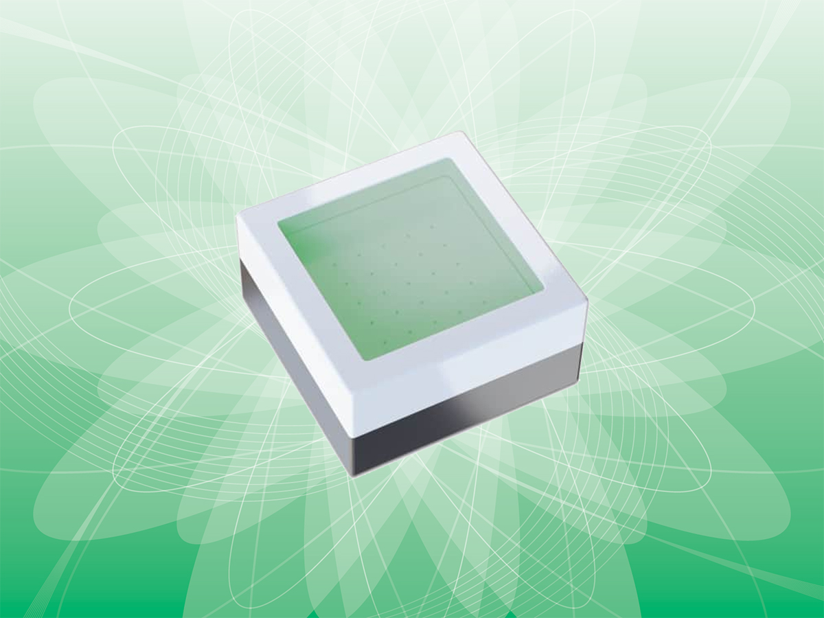
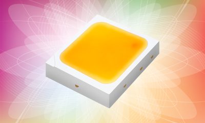
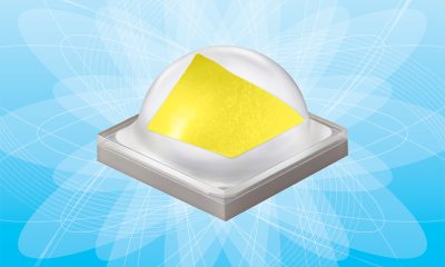
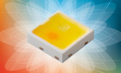
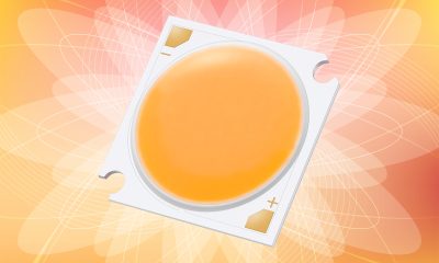
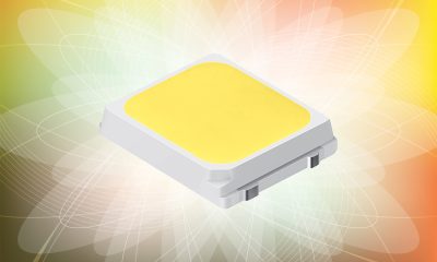
Monochromatic LED dies must be assembled into a package to before they are used in a lighting application. A semiconductor package provides interconnectivity for the LED dies to be electrically, thermally and mechanically interfaced to a printed circuit board (PCB). It also protects the dies from being damaged physically or chemically. There are a multitude of options for package design and material of construction. Generally, a color LED package includes a die carrier which may be a ceramic substrate or a lead frame. The die carrier may be embedded in a polymer housing made from silicone molding compound (SMC) or epoxy mounting compound (EMC). The LED dies and wire bonding are encapsulated in silicone. The positive and negative electrodes of the LED are commonly designed as metal pads located on the underside of the package, which improves interconnect reliability and reduces the thermal resistance between the LED die and the PCB.


Loading...