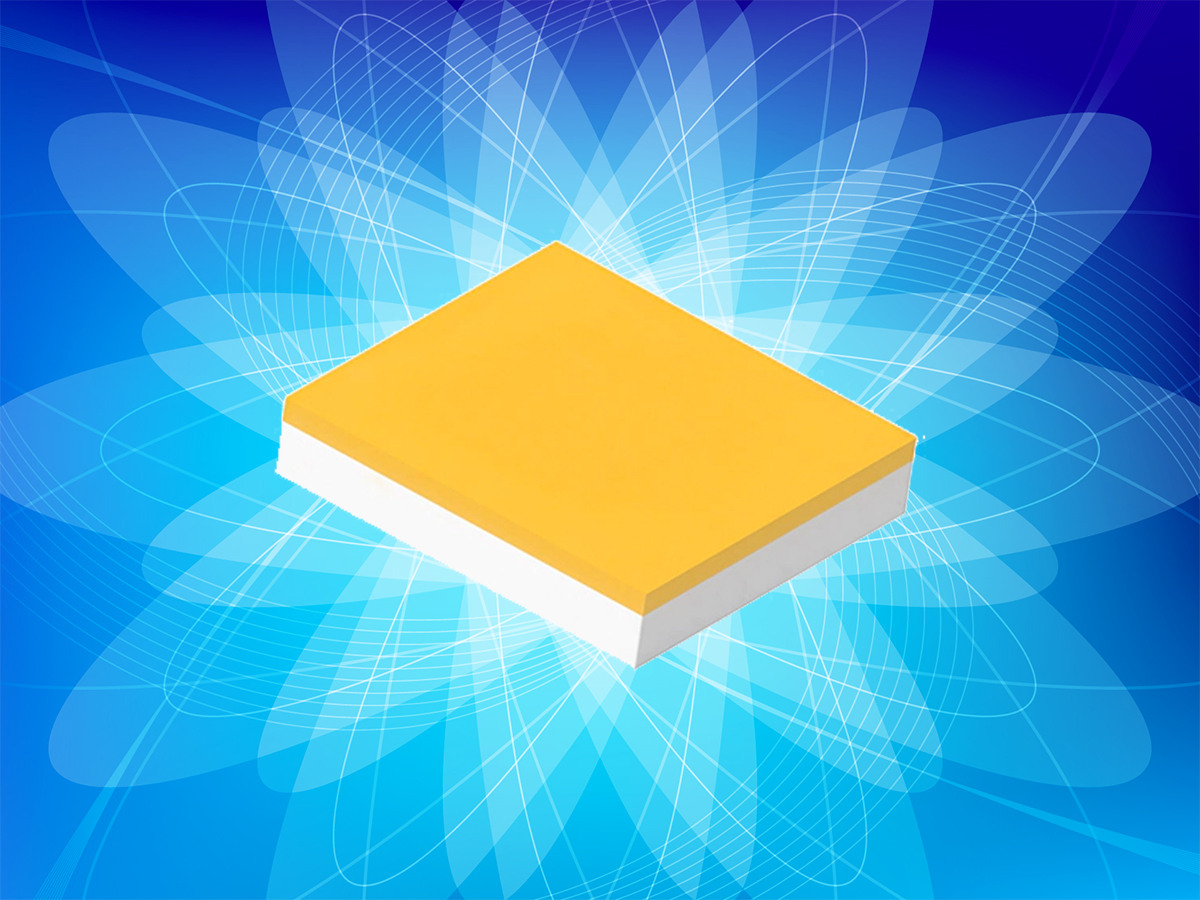
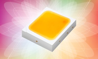
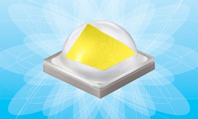
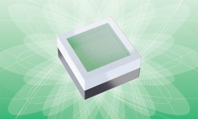
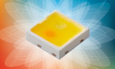
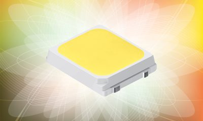
What is a high power CSP LED
A high power CSP LED is a flip-chip device that offers high drive current capability in a footprint marginally larger than its light-emitting stack. The fundamental packaging philosophy of chip-scale LED packages is to strip off superfluous package elements without compromising both thermal performance and the SMT advantages made possible with standardized packaging. In addition to significantly scaling down the package size, the CSP platform provides the benefits of greatly reduced junction-to-board thermal resistance, enhanced electrical connectivity and interconnect reliability, and a substantial reduction in material and manufacturing costs. With performance and robustness comparable to the more costly ceramic-based high power LED packages, CSP LEDs are at the heart of recent innovation in the lighting industry. CSP technology has made its way into an extensive array of applications, including high bay lighting, roadway lighting, architectural lighting, automotive front lighting, etc.
Light emission
An LED is in essence a light-emitting stack that makes use of semiconductor-based electroluminescence to produce light. It is a p-n junction formed by two oppositely doped semiconductor compound layers where positive and negative charge carriers are discharged, respectively. Sandwiched in the middle is an active region comprising at least one layer of semiconductor material. When a bias is applied across the doped layers in the forward direction, electrons in the n-type semiconductor layer are pushed into a higher state in the conduction band and holes in the p-type semiconductor layer are pushed into a deeper state in the valence band. The positive and negative charge carriers move across the boundary layer toward each other and may recombine in the active region. The recombination causes electrons to drop to a lower energy level, releasing excess energy in the form of photons. The wavelength of the emitted photons can be tuned to the visible portion of the electromagnetic spectrum.
LED packaging
A semiconductor p-n junction is commonly referred to as an “LED die” or ” LED chip. It’s not a component-level device that can be used as system constituent in an LED light. In order for an LED chip to deliver the required functionality and performance, a packaging process needs to be carried out. An LED package provides the semiconductor die the “infrastructure” for direct surface mount technology (SMT) connection to a printed circuit board (PCB), which mechanically, thermally and electrically interfaces the LED chip to its system environment. It also accommodates a wavelength converter which controls the spectral power distribution (SPD) of the emitted light to meet color specifications for a particular application. Additionally, the semiconductor package exercises control of environmental conditions to provide the chips with protection against influences of humidity, corrosive atmosphere, contaminants and thermo-mechanical stresses. The packaging design and materials of construction have a great impact on performance, color quality, lumen maintenance, chromaticity stability and reliability of a component LED.
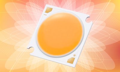
Conventional package platforms
There are a multitude of options regarding the package platform. Conventionally, an LED package comprises a carrier, an LED chip or multi-die array, and a phosphor-polymer mixture which serves as a wavelength converter and an encapsulant. Most of these device packages use wire bonding to supply power to the LED die. The carrier or submount of a conventional high power LED is a ceramic substrate made from alumina (Al2O3) or aluminum nitride (AlN), with copper filled vias providing electrical and thermal conduction paths. Metal pads on the underside of the ceramic substrate improves electrical interconnectivity as well as heat spreading into the PCB while maintaining ease of surface mounting. One of the electrodes is typically on the top of the die. A gold wire connects it to the metallized ceramic substrate. Ceramic-based high power LEDs are capable of handling high drive currents and thermal loads. They have been at the forefront of lighting applications where the need for longevity from a lighting system runs parallel with energy efficient operation and powerful lumen output. A big problem, however, is the cost. A cheaper alternative is the lead frame package based on the plastic leaded chip carrier (PLCC) architecture. High power LED packages of this type make use of epoxy mounting compound (EMC) or silicone molding compound (SMC) to improve the thermal stability of the leadframe housing. Nevertheless, long-term exposure to high temperature conditions and high-energy photons will accelerate kinetics of temperature- and photo-induced degradation of the resin material, which leads to rapid lumen depreciation and chromaticity shift.
Package design
High power CSP LEDs overcome what had been significant limitations of LED packages developed with conventional platforms. A CSP LED uses neither a ceramic substrate nor a polymer housing. It eliminates the package carrier which is either expensive or of high thermal resistance and low thermal stability. The carrier-free design offers multiple advantages, including a more compact footprint, lower thermal resistance, absence of degradation-prone materials, and a reduced cost. Another distinguishing feature of chip-scale packages is the removal of the cathode contact bond wire. Interconnect failures of LED packages related to wire bonding are catastrophic. The bond wire is susceptible to fracture during temperature cycling. The limited current-carrying capacity of the bond wire can result in an open circuit when an electrical overstress (EOS) event occurs. Environmental conditions may exert mechanical stress on the bond wire and breakages can occur. The wire-free design drastically reduces the complexity of the packaging process and drives down the cost even further. Most of all, absence of wire bonding lends reliability to the LED packages.
Die fabrication
Die construction and packaging go hand in hand. The semiconductor p-n junction of a phosphor-converted white LED is fabricated from the gallium nitride (GaN) material system. GaN as a direct and wide bandgap semiconductor can be integrated with indium gallium nitride (InGaN) to create a quantum well in which an electron can directly emit a photon when it drops down from the conduction band to the valence band upon the electron-hole recombination. GaN-based LEDs have a double heterojunction (DHJ) structure in which the InGaN active layer of only a few nanometers thick is interposed between the p-doped GaN and the n-doped GaN layers. A multiple-quantum-well (MQW) construction is usually employed to improve the quantum-confinement effect (QCE) and thus the radiative recombination efficiency (RRE). The wavelength of electroluminescence, which determines the color of emitted light, is dependent upon the bandgap of the semiconductor materials forming the MQW. The InGaN bandgap can be tuned by varying the amount of indium in the alloy and the active layer thickness.
Substrate technology
Epitaxy is the technique of atomically growing the n-GaN/InGaN/p-GaN heterojunction on a carrier wafer (die substrate). InGaN LEDs can be fabricated on different types of carrier wafers. Heteroepitaxial growth of the light-emitting stack, which is performed on foreign substrates such as silicon carbide (SiC), sapphire and silicon (Si), is the most popular technique for commercial production of InGaN LED dies. By far the most used substrate material is sapphire which allows for economical and industrially viable wafer fabrication and supports a qualitatively acceptable GaN epitaxial growth. The major downside of sapphire-based heteroepitaxial growth is the large lattice mismatch between GaN and sapphire. Lattice mismatches can introduce microcracks (called “threading dislocations”) into the crystalline structure. At these dislocations, the non-radiative Auger recombination dominates. This phenomenon has a significant impact on the LED quantum efficiency. The high dislocation density in GaN-on-sapphire LEDs is of particular concern when they’re employed in high power applications. The presence of these crystalline microcracks can accelerate defect growth under high electrical stresses and extreme thermal shocks, which can set off a chain reaction toward efficiency degradation and device failure. SiC can be used to grow high quality epitaxial films due to a number of material properties such as a closely matched crystalline lattice structure and coefficient of thermal expansion (CTE) with GaN. However, the high cost of SiC substrates has remained a challenge to the mass adoption of GaN-on-SiC LEDs. There is considerable interest in silicon substrates which are advantageous for high conductivity, large wafer sizes and low costs, but challenges of the lattice mismatch (17%) and CTE (33%) between GaN and Si are still hurdles yet to be overcome. An ideal GaN epitaxy would be homoepitaxially grown, but this approach is too expensive to be commercially viable.
Flip-chip packaging
The key enabling technology for CSP LEDs is flip-chip packaging. A typical InGaN LED die is composed of, in order, a p-doped GaN layer, an InGaN active layer, a n-doped GaN layer, and the die substrate. In the conventional high power LED architecture, the LED die is mounted in a way that the substrate sits at the bottom and light is projected outward through the p-GaN layer. In a CSP LED, however, the light-emitting stack is flipped upside down. The substrate side faces up and the p-GaN layer is at the bottom. Light is extracted through the n-doped GaN layer and the die substrate. CSP LEDs are leadless packages. The electrical leads do not extend out from the package sides. Both the anode and cathode pads of the LED are located on the base. The underlying p-GaN layer is directly interfaced to the bottom anode pad with the current flowing vertically. A portion of the p-GaN layer and InGaN layer is etched away to create vias for the epitaxial n-GaN layer to be electrically contacted by the bottom cathode pad. This configuration eliminates any need for wire-bonded electrical connection.
Device architecture
The flip-chip architecture allows the current spreading layer formed over the p-GaN layer to be made thicker so as to achieve a more uniform distribution of current density. Current spreading resistance is therefore minimized, which contributes to the drastically reduced probability of current crowding even when the LED is driven at a very high power density. At the same time, the current spreading layer spreads heat over a large surface area to reduce local heating and dissipates very high heat flux densities via the metal pad. Thermal load generated at the n-GaN layer is also efficiently dissipated as the through-hole electrical conduits are also used as thermal vias and the bottom cathode pad provides efficient interfacial thermal conduction. Among all types of LED packages, CSP LEDs have the best thermal design. The most common substrate material is sapphire which has limited thermal conductivity. In conventional package designs, this die substrate becomes an insulator between the light-emitting stack and the package submount. The flip-chip arrangement directly interfaces the p-GaN layer to the bottom electrode, thereby minimizing thermal resistance and the length of the thermal path. Both GaN-electrode interfacing and flat no-lead packaging maximize effective surface area of the thermal path.
White light generation
High power CSP LEDs produce white light through phosphor down-conversion. A phosphor-converted white LED utilizes an InGaN LED die, which produces either blue light or near-ultraviolet (UV) light, to pump a phosphor layer within the device package. The phosphor layer performs as a wavelength down-converter to spectrally shift part or all of the electroluminescence to longer wavelength light. Blue-pump LEDs have been dominating the market due to their efficacy advantage over violet-pump LEDs. These packages down-convert only a portion of the electroluminescence (blue light). The remaining amount of electroluminescence is used as primary light which is mixed with the down-converted longer wavelength light to produce white light. Compared with violet pump LEDs in which all of the emitted photons undergo the down conversion process, blue-pump LEDs suffer from less Stokes losses and therefore have a higher quantum efficiency. Despite the compromise in efficacy, violet-pump LEDs have a superior color rendering quality thank to the balanced distribution of radiant power across the visible wavelength range.
Phosphor matrix
On the whole, the correlated color temperature (CCT) and color rendering index (CRI) of a phosphor-converted white LED depend on the control of material composition and layer thickness of the phosphor down-converter. Aside from delivering the required spectrum, the phosphor and binder materials of the down-converter/encapsulation layer need to operate reliably at very high temperatures since the phosphor matrix temperature can easily be 30°C to 50°C above the LED junction temperature due to the presence of Stokes heat. The phosphor matrix is commonly applied as a conformal coating, either on all five sides of the chip or just on the top surface with side walls created by a silicone frame. To enhance light extraction, TiO2 (titanium dioxide) reflectors may be built around the side surfaces of the chip.


Loading...