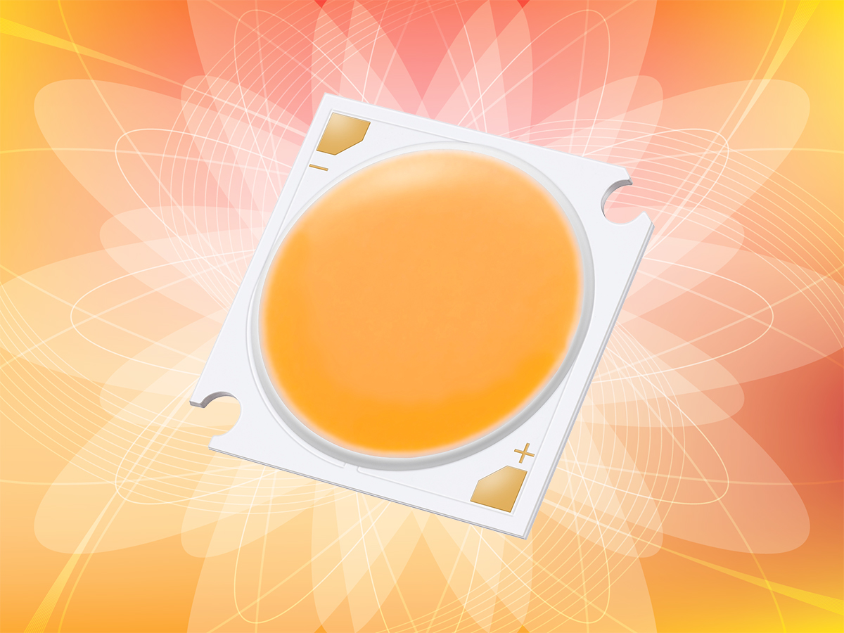
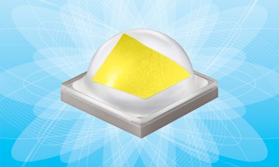
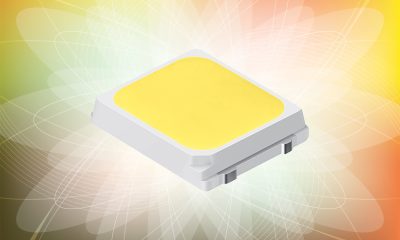
What is a COB LED
A COB LED is an integrated assembly of LED dies on a thermally conductive substrate, such as a metal-core printed circuit board (MCPCB) or ceramic. COB is an acronym for “chip-on-board”. Available in wattages of up to 200+ W, the multi-die LED array creates a light emitting surface (LES) with high flux density and high beam uniformity that is not possible with discrete high-power, mid-power, and CSP LED packages. Packing enough of a punch in the beam and designed for direct heat sink integration, COB LEDs deliver value beyond just being LED packages to simplify lighting system integration. This contrasts with SMD LED packages that have to be mounted on a printed circuit board to create the light engine. The ability to deliver powerful lumen packages and high uniformity illumination lends COB LEDs to a variety of indoor and outdoor applications. Their footprint is frequently found in high power LED systems such as high bay lights, flood lights and street lights. This type of LED packages has established its strongest foothold in directional lighting applications where a uniform beam with the highest punch possible is required. The most common use of directional lighting is for creating focal points and visual interest, which is served by accent lights such as recessed downlights, surface mount spotlights and track-mounted luminaires. COB LEDs are also incorporated in task luminaires to provide focused, localized illumination necessary to the functioning of a space.
Light emission
LEDs are complex devices capable of reaching high performances and delivering the intended value only when they’re characteristically tailored to an application and operated under controlled conditions. These devices produce light by electrically stimulating the injection electroluminescence effect in compound semiconductor structures. The basic building block for an LED is a p-n junction. It is formed by two semiconductor compound layers that are oppositely doped with impurities to exhibit different modes of electrical conductivity. There’s also a middle active region that makes up the light-emitting layer of the semiconductor emitter. When the p-n junction is biased in the forward direction, negatively charged electrons in the n-type semiconductor layer and positively charged holes in the p-type semiconductor layer move across the junction boundary layer into the active region. Light is produced as a result of energy band transition in electrons when they recombine with holes in the active region. The emitted light is a few tens of nanometers in spectral bandwidth, which appears to have a single color.
LED packaging
A semiconductor p-n junction is a light-emitting stack that needs to be mounted in a package in order for itself to work as a light source. A semiconductor package provides electrical, mechanical, thermal interfaces between the bare semiconductor die and the rest of the system. LED operation exhibits high dependency on the package’s ability to handle electrical and thermal loads. Similar to those of many semiconductor devices, the performance and lifetime of an LED are tied to its junction temperature and drive current. The package design must account for junction-to-board thermal resistance and electrical performance, and so to maintain good thermal conductivity and electrical connectivity at all times and in all operating conditions for the LED die. The package provides control over the spectral power distribution (SPD) of emitted light using a wavelength converter that shifts or spreads the narrow-band emission of the LED in wavelength. It also provides the semiconductor die environmental and mechanical protection from corrosion and physical damage. Optical design, which relates to the way to extract and direct the light into a preferable angle or distribution, must be taken into consideration as well.
Package design
The fundamental packaging philosophy of chip-on-board (COB) LEDs is to minimize junction-to-board thermal resistance, to create a surface emission device, and to simplify the process of integrating LEDs into a lighting system. An SMD LED package typically incorporates a die carrier that plays host to the light-emitting stack. A high power LED, for example, makes use of a ceramic substrate for thermal management, and a mid-power LED utilizes a silver-coated metal lead frame surrounded by a plastic cavity to create the thermal and electrical contacts to the board while improving light extraction efficiency. COB packaging eliminates the die carrier and mounts the LED dies directly onto a circuit board or ceramic substrate to create a low profile package that allows direct integration into a lighting system without the need for a separate circuit board. By stripping away the superfluous die carrier, thermal resistance and the length of the thermal path are minimized. The MCPCB or ceramic substrates also provide expanded effective surface area for the thermal path, hence the heat flow from the substrate to the heat sink is maximized. The adequately dimensioned, low resistance thermal path allows a COB package to operate with a much higher packing density than polymer-based mid-power LEDs and a much larger LES than ceramic-based high power LEDs.
Die attachment
A COB LED has an array of semiconductor dies which are often connected in a mix of parallel and series to make the LED die assembly tolerant against a single LED open or short failure. The LED array is then covered with a layer of phosphor-silicone mixture that acts as the wavelength down-converter and die encapsulant. In a conventional package design, the LED dies are wire-bonded with Au wire for electrical connection and die-bonded on the substrate with silver-filled epoxies for thermal conduction and mechanical stability. The most recent trend in COB packaging is to bump-bond flip chip dies directly onto the circuit electrodes, without resorting to the bonding wire and conductive adhesive. The current-carrying capacity and thermal conduction performance of the die interconnects define the packing density of a COB LED and affect LED performance, efficiency and lifespan. Flip chip attachment (FCA) through bump bonding presents crucial advantages for high density and high power lighting applications where a robust thermal path for each LED die must be created and high current handling capability of the die interconnects is a necessity. The reliability characteristics of a COB LED should also account for the match of the coefficient of thermal expansion (CTE) between the LED die and different package elements. A large CTE mismatch can introduce high thermo-mechanical stresses during high-magnitude thermal cycles, which can result in interface delamination and debonding.
Die fabrication
The semiconductor dies that produce pump light for phosphor converted white LEDs are light-emitting stacks constructed from a gallium nitride (GaN)-based material system. Acceptor impurity atoms are incorporated into a GaN layer to create the p-region where the majority charge carriers are positively charged holes. Donor impurity atoms are introduced into another GaN layer to produce the n-region where negatively charged electrons dominate. The p-doped GaN layer and n-doped GaN layer form a p-n junction between which the light-emitting layer (active region) made of indium gallium nitride (InGaN) is interposed. A GaN-based semiconductor light-emitting stack is a n-GaN/InGaN/p-GaN heterojunction that has high quantum efficiency in the short-wavelength region. By varying the concentration of indium in the alloy, the energy band gap of the quantum well (QW) can be manipulated such that the spectral band of the emitted photons, which corresponds to the color of emitted light, meets the needs of the intended application.
Substrate technology
The light-emitting stack is epitaxially grown on a substrate such as sapphire, silicon carbide (SiC), silicon (Si), and GaN. The most widely used substrate for GaN epitaxy is sapphire. GaN-on-sapphire LEDs are not perfect. There is a large mismatch between the crystal lattice structure of sapphire and that of GaN. Mismatched lattice structures lead to defects in the crystalline structure known as threading dislocations. The presence of the crystalline defects increases the probability of non-radiative Auger recombination, but also spurs nucleation and dislocation growth. At high operating temperatures and high drive currents, the growth of atomic defects in the active region can be accelerated and thus a shortened service life should be expected. The performance of GaN-on-sapphire LEDs at high operating temperatures and high drive currents leaves much to be desired. Very tight junction temperature control must be exercised in order for these LEDs to survive in high power lighting applications. GaN-on-SiC and GaN-on-GaN LEDs offer a higher quantum efficiency than GaN-on-sapphire LEDs. They are much more robust in high temperature and high power density conditions due to the high quality GaN epitaxial growth. However, they fell at the hurdle of high manufacturing costs.
Flip chip attachment
Flip chip attachment drives a fundamental improvement to the design of COB packages. In conventional package architectures, the substrate where the light-emitting stack is epitaxially grown is at the bottom of the LED die. Light passes through the p-GaN layer which is at the top of the active region. Wire bonding is imperative in order to create the electrical contact for the p-GaN layer. Wire bonding represents a single point of failure (SPOF). The current-carrying capacity of the bond wire is often inadequate to withstand an EOS event. The thin wire is also subjected to thermo-mechanical stresses. The insulating nature of the sapphire wafers results in a high junction-to-board thermal resistance. The FCA technology eliminates wire bonding and puts the epitaxial p-GaN layer down on the package substrate. Direct bonding between the p-GaN layer and package substrate facilitates heat spreading. Wire-free electrical connection removes the bottleneck that affects current flow and the EOS robustness. Enhanced electrical, thermal, and mechanical interconnectivity translates to high power density capability of the individual LED dies and high die density (packing density) of the LED package.
White light generation
A major role of LED packaging is to spectrally optimize light emitted by the LED die which emits in a narrow spectral band representing a single color rather than a polychromatic white. Phosphor down-conversion is the most commonly used strategy to broaden the narrow full width at half maximum (FWHM) of LED dies and achieve white light. An LED package use phosphors to partially or completely convert the electroluminescence to broad-spectrum light. The vast majority of commercial white LEDs utilize blue light emitted by InGaN dies to pump phosphors within the device package. The phosphor down-converter absorbs a portion of the electroluminescence (primary light) and then shifts and spreads it to create longer wavelength photons. The down-converted photons mix with blue photons that don’t participate in the down conversion process to create white light. COB LEDs can also use ultraviolet-producing InGaN dies and a down-converter containing red, green and blue phosphors to produce white light. These violet-pump LEDs outperform blue-pump LEDs by wide margin in terms of color quality. Full wavelength conversion contributes to a spectral power distribution (SPD) that is uniformly spread throughout the visible spectrum, which lends the LEDs the ability to reproduce the colors of illuminated objects faithfully. However, the luminous efficacy of violet-pump LEDs is inevitably lower than blue-pump LEDs due the large Stokes energy losses occurred during the down-conversion process.
Phosphor matrix
A COB LED can be characterized by its correlated color temperature (CCT) and by its color rendering index (CRI) or a color rendering metric produced by an alternative metric system. Accurate delivery of these color characteristics requires careful control of the down-converter’s material composition and layer thickness. The inclusion of phosphors into a COB LED package must account for their particle size, concentration, geometry, carrier medium, thermal stability, quantum efficiency, and refractive index matched with the encapsulant material which is usually silicone. The silicone/phosphor mixture is applied to a COB LED package by dispensing. Uniform distribution of phosphor particles in the silicone matrix and uniform layer thickness over the LED dies are critical to the color angular uniformity of the LES and reproducible white chromaticity points in production. The COB packaging architecture results in a very high thermal stresses on the phosphor and matrix materials due to the combined forces of power dissipation from the LED junction and the Stokes heat generated by the phosphor down-converter. The thermal performance of the phosphor layer should be carefully evaluated. When the thermal load at the phosphor layer is too high to be properly dissipated by the semiconductor package, the use of a remote phosphor may be the only solution.
Package submount
Ceramic substrates are used in COB packages which produce a thermal load with a high heat flux density. With superior thermal conductivity, electrically insulative property, and high thermal and chemical stability, ceramics have every qualification for LED thermal management. However ceramic substrates are expensive and too brittle to allow for assembly and handling with ease. Compared with ceramic substrates, MCPCB substrates are less expensive and support ease of use, though their relatively lower thermal conductivity is a disadvantage. The most common MCPCB construction consists of an aluminum or copper substrate at the bottom, a thermally conductive dielectric layer in the middle, and a top copper layer. The performance of MCPCBs largely depends on the construction of the dielectric layer which should preferably have high thermal conductivity, high insulation resistance, high decomposition and glass transition temperatures.


Loading...