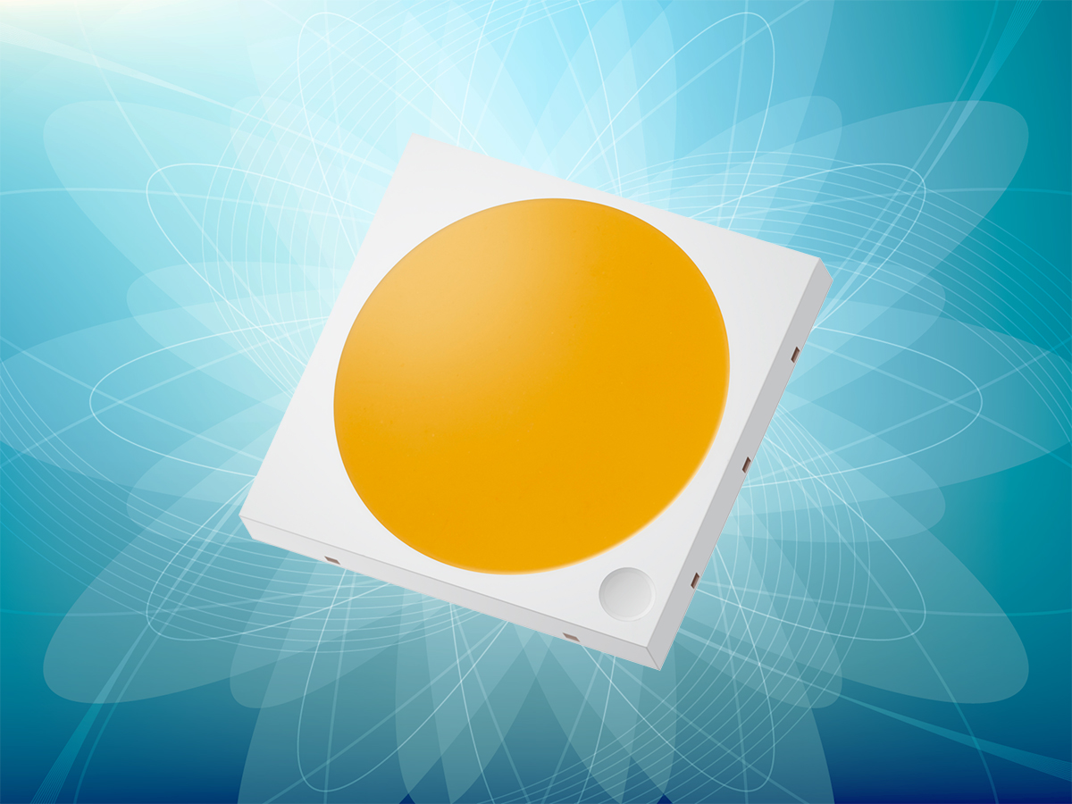
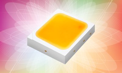
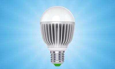
What is a high power lead frame LED
A high power lead frame LED package is a polymer-based, multi-die semiconductor emitter that builds upon the plastic leaded chip carrier (PLCC) architecture. The LED emitter comes mostly in an industry standard 5050 surface mount package. High power LEDs of this type are made to harvest the high efficacy advantage of reflector-based SMD packages. Improvements in thermal path design and the use of high operating temperature capable housing materials afford these LEDs the ability to operate at higher junction temperatures and drive currents. However, the inherent limitations in the package platform challenge their dependable performance in applications that are served by conventional ceramic-based high power LEDs and the rapidly adopting CSP LEDs. In general, high power lead frame LEDs are intended for use in controlled environments or cost-sensitive projects. Their footprint can be found in both indoor and outdoor lighting systems including high bay lights, low bay lights, flood lights, high mast lights, street lights, landscape lights, architectural and facade light fixtures, etc.
Light emission
An LED is basically a p-n junction which is built by joining together two semiconductor layers having different modes of electrical conductivity: the N-type semiconductor layer and the P-type semiconductor layer. The p-n junction comprises an active region of semiconductor material interposed between the two semiconductor layers. When a p-n junction is biased in the forward direction, negatively charged electrons and positively charged holes move across the boundary layer toward each other and recombine in the active region. Recombination of an electron and hole results in energy level transition in the electron from the conduction band to the valence band, with the lost energy released as a photon. The frequency of the photon is determined by the semiconductor bandgap, which is the difference in energy between the conduction band and valence band. The semiconductor bandgap can be manipulated such that a photon can deliver electromagnetic radiation in the visible wavelength range. This electrically stimulated emission of visible light in a solid state device is known as electroluminescence.
LED packaging
The p-n junction is a semiconductor die that merely provides a physical mechanism for electroluminescence. Electroluminescent devices by nature are very complex. They operate under specified ranges for electrical power and require thermal management to keep the junction temperature within prescribed limits. When used as white light sources, the narrow-band emissions from the semiconductor die must be broadened to deliver the required spectrum. Therefore, the p-n junction semiconductor die has to be integrated into a device package that allows itself to be thermally and electrically interfaced to the operational environment while providing enhancements in light spectrum and addressing other needs. In the LED industry, the p-n junction is called an LED die or LED chip. The term “LED” typically refers to an LED package. A LED package can perform a variety of functions and deliver a number of benefits. It provides the chip with interconnects for electrical supply, heat dissipation and mechanical support, incorporates a wavelength converter to optimize the spectrum, helps extract and direct the light into a preferable angle or distribution, and protects the chip from environmental contaminants.
Package construction
In a high power PLCC LED package, an array of LED dies are mounted on a lead frame by means of a solder bond or conductive glue. The lead frame performs as a carrier substrate to support the LED dies, creates one of the two electrical contacts connecting the dies to the external circuit, and provides a thermal pathway to conduct heat away from the LED junction. Wire bonding is used for the connection to the second contact pins of the LED dies. The lead frame is embedded in or surrounded by a plastic housing made from a resin. The cavity of the housing is filled with a phosphor-polymer mixture which acts as the down-converter and encapsulant. Normally, highly reflective silver plating is applied the lead frame. (Nevertheless, sulfur-containing compound can react with silver-plated lead frame surfaces to form silver sulfide. The lead frame may become discolored, which leads to chromaticity shifts and reduced light output. In extreme cases the corrosion can result in an open contact. In contrast, gold plating offers higher chemical stability but is less reflective.) The polymer housing also provides a reflective cavity. With both lead frame and housing acting as reflectors, the LED package is able to extract as much of the light generated by the dies as possible. High efficiency light extraction is the distinguishing ability of plastic LED packages. It allows the old package platform to gain a solid foothold in mid-power LED packaging and make its way into high power applications.
Housing material
While high power packages share a lot common with the mid-power counterparts, they must overcome the limitations of the PLCC architecture in order to survive operational stresses at high operating temperatures and drive currents. Conventional polymer-based LED packages have poor lumen maintenance and color stability due to degradation of the plastic resin under thermal and photooxidative stresses. Common polymers used for making LED package reflectors are thermoplastic resins including polyphthalamide (PPA) and polycyclohexylenedimethylene terephthalate (PCT). PPA is almost the universal choice in mid-power LED packaging applications because of its low cost and high reflectance 95%) in visible wavelength spectrum. However, PPA is particularly prone to thermal degradation and photo-oxidation, which limits its use in LED packages with power dissipations of around 0.5 W or less. PCT has moderately higher performance but cannot afford device operation at 0.7 W or a higher wattage. Discoloration of PPA and PCT resins is a dominant color shift mechanism in mid-power packages and simultaneously results in significant lumen depreciation due to light absorption by the sidewalls. High power packages are constructed from thermosetting resins that have higher stability compared with PPA and PCT. Epoxy mounting compound (EMC) is typically used in LED packages a power consumption of around 1 W. Silicone molding compound (SMC) is a necessity in products operating under more intensive thermal stresses.
Interconnects
Conventional PLCC LED packages are highly susceptible to electrical overstress (EOS) and thermal stresses due to the device structure on the part of current and heat spreading. Electrical leads are usually wrapped around to the base of the package for surface mounting onto the PCB which electrically and thermally connects the LED package to an external circuit. Solder joints are one of the key determinants of power density, thermal performance and reliability of LED products. With the lead-type interconnects, the integrity of the LED substrate to PCB solder joint can be easily compromised due to strains incurred in thermal cycling, high frequency of on/off power cycling, electrical metallurgical interdiffusion and electrostatic discharge. High power LED packaging makes use of Quad Flat No-leads (QFN) interconnects to address these problems. A QFN LED has planar copper lead frame substrates located on the base of the package. The anode and cathode pads provide dramatically increased interface area for heat and current spreading, which imparts high reliability, high operating temperature and drive current capable interconnectivity to an LED lighting system.
Die fabrication
The LED die that is assembled into high power white LEDs is fabricated from gallium nitride (GaN). The semiconductor has a direct band gap which contributes to a higher probability of radiative recombination than semiconductors with an indirect band gap. A GaN-based LED has a double heterojunction (DHJ) structure. The die of a PLCC type package has a n-doped GaN layer at the bottom and a p-doped GaN layer at the top. The active region between sandwiched between the two oppositely doped layers is grown with different concentrations of indium gallium nitride (InGaN) to create a quantum well (QW) based light-emitting) layer. The multiple-quantum-well (MQW) structure is used routinely in most GaN-based LEDs because it can confine more charge carriers to achieve a higher carrier radiative recombination efficiency (RRE) than a single quantum well (SQW).
Substrate technology
The n-GaN/InGaN/p-GaN MQW heterostructure is grown on a carrier wafer which is commonly known as a substrate. Heteroepitaxial growth of GaN on sapphire remains the key enabling technology for die fabrication due to its high processability and mass production viability. However, growing GaN semiconductors on foreign substrates leads to a lattice mismatch between GaN and these substrates. A large mismatch between the crystal lattice structure of the light-emitting stack and that of the substrate results in a high density of threading dislocations (microcracks) in the epitaxial films. Electron-hole recombinations that take place at sites of crystalline defects are primarily “non-radiative,” which means a reduced probability of photon generation and hence a lower internal quantum efficiency (IQE). The crystalline defect generation and growth can be accelerated with the increasing operating temperatures and drive current density. This makes a very adverse effect on high power applications. A sapphire substrate has ~16% lattice mismatch with GaN, which is considerable large. One technically successful alternative is silicon carbide (SiC) which more closely matches the GaN lattice structure (3.4% lattice mismatch). A SiC substrate not only creates fewer dislocations, but also has higher thermal conductivity and better resistance to electrostatic discharge. An ideal substrate for GaN epitaxy, however, will be homoepitaxially grown on a high quality GaN wafer itself. Homoepitaxial growth of GaN makes technical sense but costs of such devices are indeed large.
White light generation
As a light-emitting stack, the semiconductor die emits light in a narrow spectral range. The bandwidth of the spectral power distribution (SPD) of bare LEDs is typically between about 10 nm and 30 nm. The wavelength of emitted light and thus the color of the light are essentially determined by the band gap energy of the materials forming the active region. The monochromatic light needs to be converted to a polychromatic white light through phosphor down-conversion which transforms shorter wavelengths into longer ones through a mechanism known as the Stokes shift. Partial down-conversion is the most common strategy to achieve white light because, compared with the full down-conversion strategy, the Stokes shift is relatively smaller and consequently there’re less energy losses. Phosphor-converted LEDs are commonly blue-pump packages which can simultaneously achieve the efficacy and cost targets. For color-critical applications, phosphor-converted LEDs that employ complete conversion of electroluminescence will be better candidates. In these packages, phosphor down-conversion is accomplished by using a near-ultraviolet (UV) LED die to pump three separate RGB phosphors. The result is a spectrum with uniformly distributed radiant power over the entire wavelength range, which lends high color rendering performance to the LEDs. As expected, this ability comes with the price of a penalty in luminous efficacy.
Down-converter and encapsulant
The phosphor down-converter is uniformly dispersed in the polymer encapsulant prior to being deposited over the LED die. At present, all of the high power LED packages use silicones as the matrix for phosphor encapsulation. Silicone polymers are easily miscible with a phosphor powder and the transparent solid matrix after the liquid-solid transition upon cure has high optical transparency, structural stability during service and mechanical softness for preservation of wire bond. Most importantly, silicone is more stable than epoxy against thermal degradation and photo-oxidation. The high-power LED architecture often produces the most thermal stress to the phosphor and the encapsulating polymeric materials because of the large amount of Stokes heat generated during the wavelength down-conversion process. To maximize light extraction efficiency, refractive Index (RI) mismatch between the silicone matrix and phosphor particles must be closely matched. A large RI mismatch will lead to a high efficiency loss due to light scattering and total internal reflection (TIR).


Loading...