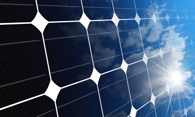
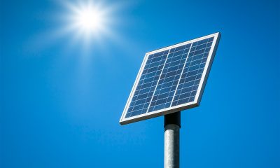
A thin film solar panel is a photovoltaic module that is fabricated on an extremely thin semiconducting absorber layer. Thin film solar panels use a very small amount of semiconductor material to convert light directly into electricity using the photovoltaic effect. The thickness of the semiconductor material is generally 5 microns or less, or about 20 times thinner than a single crystal silicon or polycrystalline silicon wafer. Accordingly photovoltaic devices are classified into bulk type that requires considerable silicon material and thin film type that consumes much less photosensitive material. Conventional monocrystalline and polycrystalline solar cells belong to bulk type.
Thin film solar panels are made by depositing one or more thin layers of semiconductor material onto a substrate, such as glass, plastic or metal. The semiconductor compound used to make these panels can be amorphous silicon (a-Si), cadmium telluride (CdTe), copper indium gallium diselenide (CIGS), and gallium arsenide (GaAs).
Amorphous silicon (a-Si) is the non-crystalline form of silicon usually fabricated by a technique called plasma-enhanced chemical vapor deposition. This technology offers cell efficiencies of 5%–7% (single junction) and 8%–10% (double- and triple-junction). Amorphous silicon cells are less sensitive to temperature but can experience a significant drop of about 10 to 30 percent during the first six months of operation.
Cadmium telluride (CdTe) was introduced to improve the low efficiency experienced with amorphous silicon. CdTe thin film solar panels have an average efficiency between 7% – 12% and have maxed out at 16.5%. Improved efficiencies combined with the ease of preparation make CdTe solar modules by far the most successful photovoltaic thin-film technology. CdTe solar panels have a considerably good performance in high temperatures and in low-light conditions. The disadvantages with using CdTe in photovoltaic applications is the limited supply of tellurium and toxicity of cadmium.
Copper indium gallium deselenide (CIGS) is a quaternary material that has a high optical absorption coefficient. This ability gives thin film solar panels the potential to approach crystalline silicon panels in efficiency. Typical energy conversion efficiency of CIGS solar panel ranges from 10% to 15%. Higher efficiencies (over 20%) have been also reported. High efficiency, extremely thin film (1.5–2 μm), the ability to adjust band gap, and a thermal and chemical stability make CIGS a front-runner in thin film technologies. However, CIGS solar panels are currently ruled out due to their expensive price and availability.
Gallium arsenide (GaAs) is a group III-V semiconductor with a band gap of about 1.4 eV. The nearly ideal band gap for solar energy conversion allows GaAs thin film solar panels to deliver the highest efficiency among all technologies. The efficiency of GaAs solar panels ranges between 20% and 25%, with a record near the 30% mark. GaAs solar panels are used in high-value applications such as space exploration where a higher electricity output is required. GaAs photovoltaic modules are resistant to radiation damage and have excellent heat tolerance and high temperature performance. However, GaAs solar panels are too expensive for common consumer applications.
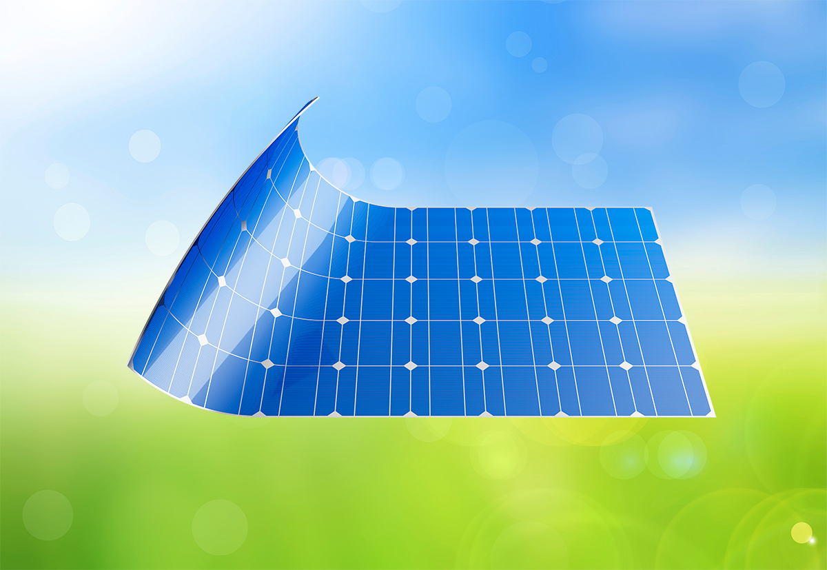
The major advantages of thin film solar panels over crystalline silicon panels are related to the facts that have a lower production cost, consume less raw materials, and can be made lightweight and flexible. Another competitive edge is that thin film panels do not lose as much efficiency as their temperature increases and they usually perform better in shade or low light conditions.


Loading...